|
CS223
Survival Guide for FPGA and Verilog Labs
| |||||||||||||||||||||||||||||||||||||||||||||||||||||||||||||||||||||||||||||||||||||||
THE FAMOUS TUTORIAL LINKThe tutorial for Xilinx ISE11 is right here (Bilkent Mirror) or original link (Xilinx Mirror). The tutorial covers almost everything explained on this page. You need to read that before attempting your labs (Pleaseeee....).You may check these links too: Xilinx Tutorials page ISE Quick start guide iSim user's guide iSim in depth tutorial HOW TO INSTALL XILINXI won't mention much here, probably just straigtforward, but here are some notes:-Run "Xilinx_11.1_ISE_DS_SFD\xsetup.exe" to install XilinxISE (where we realize and create our projects); -Run "Digilent\DAS(x86)2-1-0.exe" to install drivers and programming software for your BASYS2 board. If you won't download your solution to your board, you won't have to install this one. While installing, Xilinx, select "Web Pack" as this is the free one. After the installation finishes, continue with the license manager to get a license for the web pack suite (its free but it still requires a license). It may also require you to create an account on xilinx web site, however I see that it is only for their records, as soon as I selected the WebPack, it setup all the necessary license settings, it seems that you don't have to login on the Xilinx web site, but you may want to create an account and continue with the web page to be on the safe side. Web page says your license is installed, after you enter your address information. Again, while installing Xilinx, it will ask to install some cable drivers, it is OK to allow that too (and probably necessary if you want to use your FPGA board). TroubleshootingThere are some problems with some individual computers which might be related to the operating system or some other unknown factor. Up until now, we have encountered the following problems while installing and running Xilinx:-When running xilinx, whenever "New Project" or "New Source" menu item is selected, the program crashes. We don't have a working solution for this problem, but we have been suspecting that it occurs because of system resources are running low. Try to close running programs and background processes that might be running on your pc, then try again. We are still trying to find a permanent solution for this problem. Update: This seems to be a memory related problem, in most of the cases closing processes from the task manager solved the case. -When trying to install DAS(Adept) software, it says "Incorrect name" or something similar, and won't launch. We are still trying to find a solution for this problem. If this is your error, you may consider using the computers in the lab to transfer your 'bit' file into the basys device. -When trying to run DAS(Adept) software, it says "missing dll file" and does not start. This problem might be caused if you have installed 32-bit ADEPT software on a 64-bit operating system. If this is the case you can download the 64 bit version of the ADEPT software from the DIGILENT web site (64-bit). There are also some cases that this problem can be seen on a 32 bit operating system, which we don't have a quick solution yet but suggest you to install properly from a setup file which can be downloaded from DIGILENT web site (32-bit). If you still cannot manage the problem, the best thing to do would be to use one of the lab computer in this case. -When trying to generate programming file, an error related with "Bitgen not started" properly may come up. This case only occurs if you have started the 30 day trial license. You can solve this problem by launching the license manager (Start --> Xilinx Ise Design Suite 11 --> Manage Xilinx Licenses) then select "Acquire a License" from the top, then select "Start ISE WebPack" then click "Next" and "OK" then "Close". After this there should be no problems on generating the programming file. -If you cannot let your operating system to identify your device, make sure you have: -installed the correct ADEPT software for your operating system (32 bit/64 bit); -removed and inserted the device with its power switch on; -restarted your computer; -tried a different usb port. -If you have programmed the FPGA but it doesn't seem to be working at all (not responding anything) and you are sure that you do nothing wrong, you may want to check the PC/ROM jumper on the device itself. When you are programming it make sure the jumper is in "PC" mode (turn off the device while changing the jumper settings). HOW TO START A PROJECTTo start XILINX, select "Start Menu --> Programs --> XilinxISE Design Suite 11 --> ISE --> Project Navigator"The following is a set of screenshots that shows how to start a new project.< Select File-->New Project... 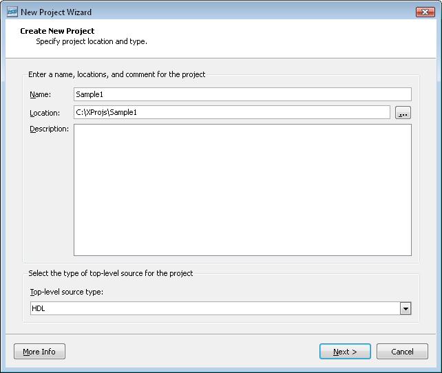 Select Next. There are certain settings that should be selected when creating a new project. Make sure that the following items are selected on the "Create New Project" screen. Family:Spartan3E 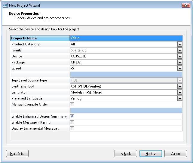 You can create a new source file from this point, or you can add from the Project menu. Select "Schematic" if you want to realize your design using a circuit schematic or select "Verilog Module" if you want to write verilog code for your system.  This is it, now you are ready to implement your designs. HOW TO GENERATE "BIT" FILEA bit file is all of your design, codes and etc, to be loaded into a FPGA board. This is the file you fill program your BASYS2 board with. After entering all your schematics or your codes, select your resource file (verilog module or schematic) from the files window, then just double click on the "Generate Programming File" from the tasks list. It will run all the necessary tasks to do that, and if it succeeds, there will be a green tick near the task. If there are any errors or warnings you can similarly see it with the icons on the task list and check necessary logs to see what has gone wrong. If you can see a green checkmark near the "Generate programming file" task, then your "bit" file is ready to be uplodad into your FPGA board, residing on the root folder of your project. HOW TO DEPLOY YOUR PROJECT TO BASYS2 FPGA BOARDDon't worry if this becomes a nightmare, if you are already on this step, you probably have solved many incomprehensible conflicts and problems.There are two possible approaches to start this phase. You can use a user interface with PlanAhead software (already installed with Xilinx) or you can just go with the manual editing (sometimes this one is a better solution). Manually editing the ucf file Sometimes editing a ucf file by hand is the best, and sometimes you need to solve some errors that might come on generating the programming file. First create a ucf file described in the approach 1 or select "Tools --> Constraints Editor" (which will create a new ucf file for you with the same name as your verilog file or schematic file, also that file must be selected beforehand). After you have a ucf file, you can select it and from the task list, double click on "User constraints --> Edit constraints file (Text)". This will open the ucf file in a text editor and you can write your input outputs and associated pins as shown below. The following is the contents of a ucf file with sample input outputs:
After creating and filling in the ucf file, you can generate the programming file and upload your bit file into your BASYS2 device. But first right click on "Generate Programming File" and select "Process properties...", this will open a new window. Select "Startup options" on the left and select "JTAG Clock" for the "FPGA Start-up clock" proprty. Click "OK" and close the window. After this part, make sure you have a green checkmark on "Generate programming file" task, if not, check "How to generate bit file" section on this page (or just double click on it). Then open your Digilent Adept program; 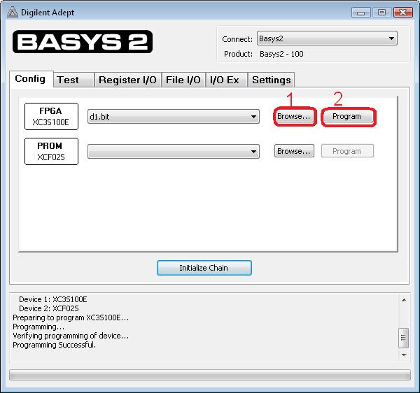 Select "Browse for the FPGA section, and locate your ".bit" file which should reside on the root folder of your project. Then select "program" button and if you see a "programming successful" message at the bottom, then you are finished. Congragulations... BASYS2 USER GUIDE & PIN LAYOUTClick here to download Basys2 User Guide (PDF)NOTE: On FPGA board SW0 is marked with M4, same as BTN2. Correct PIN idenfiters are shown in the table below (which are SW0-P11 and BTN2-M4) 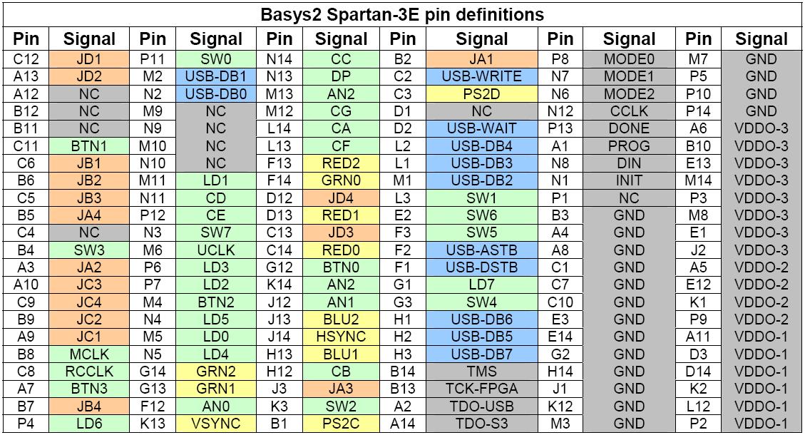 For those who wish a summary table, its right here: (These are the ones we will be using at most, BUT you can also follow these from the board itself)
Seven Segment outputs will be added on a later update, with its own article. Don't worry about the MCLK right now, it will be used later. SWx stands for a switch, its right on the lower lefthand side of the board. There are 8 switches named SW0 to SW7. 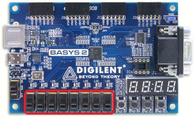 BTNx stands for a button. Its on the lower righthand side of the board (below seven segment displays). There are 4 buttons named BTN0 to BTN3. 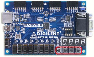 LEDx or LDx stands for a LED. Its just over the switches. There are 8 leds named LD0 to LD7. 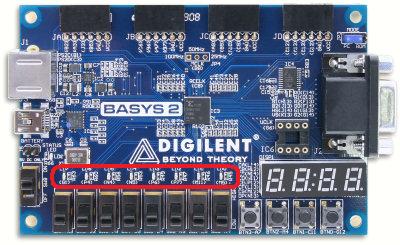 THE MISSING VERILOG SAMPLESHere are the files for verilog samples (in case you cannot find the files from the course web page):
HOW TO USE ISIM? (Simulation)For simulating your designs you need a test bench file. After writing your verilog module, select your module from the design window, right-click on it then select "New Source...". After this select "Verilog Test Fixture" and continue as if you are adding a new verilog file. Just one important note, it will ask which verilog modules you want to associate this test fixture with, and you need to select the modules you want to test at that point.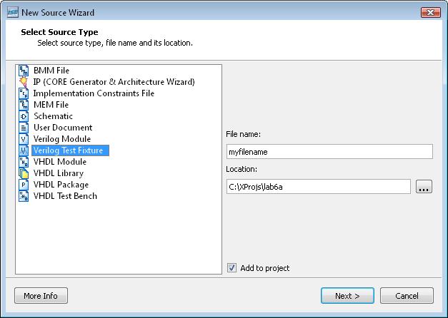 The newly created verilog test fixture will be shown as a new document. In this document you can write your test codes as shown below. For illustrative purposes, initially 4 inputs will be set to 0 then after 100 nanoseconds A and B inputs' first bits will be changed to 1. Only the code in the red rectangle is added by the user in the screenshot below. 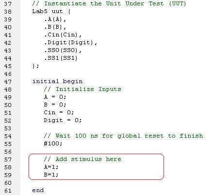 Next step is to select "Behavioral simulation" from the design window, select your test fixture file, then select the "Simulate Behavioral Model" on the task list. 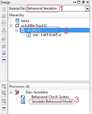 This will open the iSim window where you can see your simulation results and many more information which will help you to debug your code and circuit. 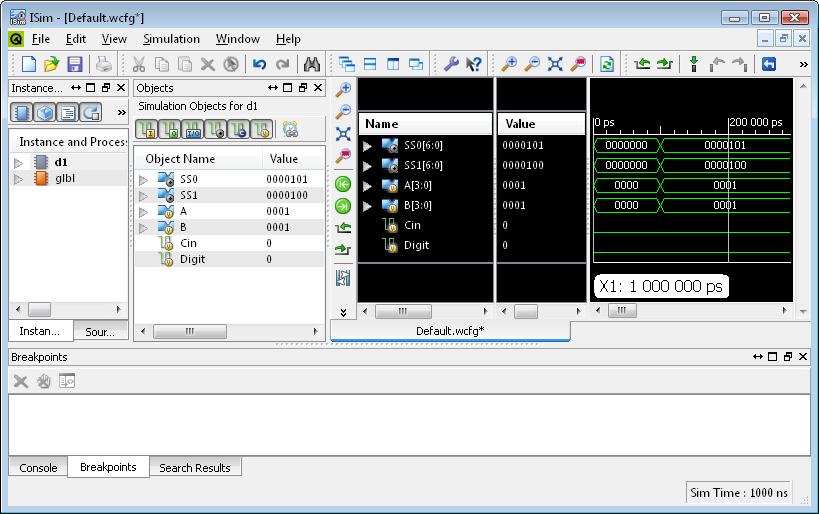 To learn how to use iSim please read the iSim user's guide document and iSim in depth tutorial documents. PS: For those who have taken this course before might wonder where is the "Test bench waveform editor" has gone, unfortunately, starting from Xilinx version 11.1, Test Bench Waveform Editor and test bench waveforms are no longer supported. More information can be found here. HOW TO USE SEVEN SEGMENT DIGITS?Seven segment ports are shown below.NOTE: On FPGA board AN0, AN1, AN2, AN3 seem to be marked incorrectly. Correct PIN identifiers should be AN0(K14), AN1(M13), AN2(J12), AN3(F12) (please notify me if I'm wrong on this one) 
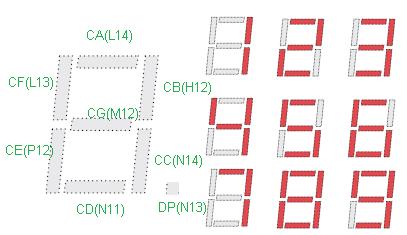 One thing to note is that all of the seven segment ports are active-low. In other words, if you want to light up any selected segment, you need to set its value to "0". For example, if you want to show a "2" in seven segment output, you need to set its inputs from A to G as such: "0010010" (i.e. the inverse of "1101101"). Also if you want to select the first digit, you need to set the anode inputs as "1110" (i.e. the inverse of "0001"). The tricky part for the seven segment outputs can be seen then you want to output more than one digits. It is only possible if you have a clock in your system. If you don't have one, you can only display one digit at a time (or same 1-4 digits of the same "digit value" on all of the digit outputs at the same time, 1111,2222,3333, etc.). The simple case, displaying one digit -Output AN1 AN2 AN3 AN4 to select one (or more) digit of your choice. Outputting {AN1,AN2,AN3,AN4}={1,1,1,0} will select the last seven segment digit. Outputting {AN1,AN2,AN3,AN4}={0,0,1,1} will select the first two seven segment digits (they will display the same value). -Output CA1..CA7 to select the segments. Outputting {CA,CB,CC,CD,CE,CF,CG}={0,0,1,0,0,1,0} will output a "2" number on the selected sevensegments. All other digits must be manually selected and displayed (be careful about the inverted inputs of seven segments). The complex case, displaying more than one digits each showing different values You need a clock for this case to work. The idea is same with a single digit, but this time you have to differentiate your outputs based on time. In other words, you will display the first digit for some time interval, then you display the second digit for some other time interval, and display the third and forth in each seperate time intervals. If this time interval is really small, the human eye will not notice the sequence of the digits and will observe all digits are displaying at the same time. This is the reason for a clock. On our BASYS2 boards we have a clock of 50 Mhz (which can be altered to 25 MHz or 100 Mhz via a jumper, see documentation). This means the clock will alternate its output 5 000 000 times in 1 second. So if you are to count the clock output change, you can count up to 5000000 and say that 1 second has passed. For the seven segment to work we need to count up to a smaller value (if we were to display each digit for one second our eyes would notice the output flickering). So count up to 100 000 is a good value with a 50Mhz clock. In 400 000 clock cycles, display your first output in the first 100 000 clock cycles, display your second digit in the second 100 000 clock cycles, display your third digit in the third 100 000 clock cycles and lastly, display your last digit in the last 100 000 clock cycles. By this way, you would have your 4 digit seven segment output. By exercising on this concept, you will find your own ways to implement on seven segment digits properly (writing a module to output seven segments, etc). |